 | –≠–ª–µ–∫—Ç—Ä–æ–Ω–Ω—ã–π –∫–æ–º–ø–æ–Ω–µ–Ω—Ç: LTC1642 | –°–∫–∞—á–∞—Ç—å:  PDF PDF  ZIP ZIP |
1
LTC1642
Hot Swap Controller
May 1999
Final Electrical Specifications
Information furnished by Linear Technology Corporation is believed to be accurate and reliable.
However, no responsibility is assumed for its use. Linear Technology Corporation makes no represen-
tation that the interconnection of its circuits as described herein will not infringe on existing patent rights.
DESCRIPTIO
U
The LTC
Æ
1642 is a 16-pin Hot Swap
TM
controller that
allows a board to be safely inserted and removed from a
live backplane. Using an external N-channel pass transis-
tor, the board supply voltage can be ramped up at a
programmable rate. A high side switch driver controls the
N-channel gate for supply voltages ranging from 2.97V to
16.5V.
The SENSE pin allows foldback limiting of the load current,
with circuit breaker action after a programmable delay
time. The delay allows the part to power-up in current
limit. The CRWBR output can be used to trigger an SCR
for crowbar load protection after a programmable delay if
the input supply exceeds a programmable voltage. The
RESET output can be used to generate a system reset with
programmable delay when the supply voltage falls below
a programmable voltage. The ON pin can be used to cycle
the board power. The LTC1642 is available in the 16-pin
SSOP package.
s
Single Channel Positive NFET Driver
s
Programmable Undervoltage and Overvoltage
Protection
s
Foldback Current Limit
s
Adjustable Current Limit Time-Out
s
Latch Off or Automatic Retry on Current Fault
s
Driver for SCR Crowbar on Overvoltage
s
Programmable Reset Timer
s
Reference Output with Uncommitted Comparator
s
V
CC
: 2.97V to 16.5V Normal Operation, Protected
Against Surges to 33V.
s
16-Pin SSOP Package
s
Hot Board Insertion
s
Electronic Circuit Breaker
APPLICATIO S
U
, LTC and LT are registered trademarks of Linear Technology Corporation.
FEATURES
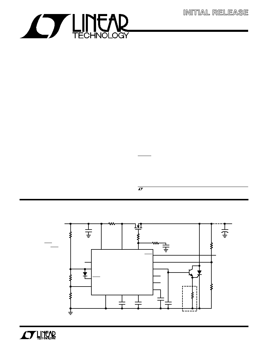
TYPICAL APPLICATIO
U
Hot Swap is a trademark of Linear Technology Corporation.
12V
V
CC
SENSE
GATE
GND
BRK TMR
LTC1642
RST TMR
16
15
14
8
2
3
COMPOUT
ON
FAULT
OV
10
4
6
9
RESET
FB
CRWBR
COMP
+
REF
COMP
≠
5
7
1
11
13
12
C3
0.33
µ
F
C2
0.33
µ
F
C5
0.1
µ
F
Q2
2N2222
Q3
MCR
12DC
D1
1N4148
R6
2.87k
1%
R5
110k
1%
R2
100
5%
R3
107k
1%
R4
13k
1%
R9
220
5%
Q1
FDR9410A
C6
0.01
µ
F
C1
0.047
µ
F
C
LOAD
12V
AT 2.5A
R8
330
5%
R1
0.010
5%
R7
11.3k
1%
POWER-GOOD = 11.4V
1642 TA01
LATCH OFF: FLOAT FAULT
AUTOMATIC RETRY: TIE FAULT TO ON
RESET TIME = 200ms
CURRENT LIMIT TIME = 20ms
CROWBAR TIME = 90
µ
s
UNDERVOLTAGE = 10.8V
OVERVOLTAGE = 13.2V
+
C7
0.1
µ
F
R9 REQUIRED ONLY WITH SENSITIVE GATE SCRs,
NOT NEEDED WITH MCR12
2
LTC1642
Supply Voltage (V
CC
) .................................≠ 0.3V to 33V
SENSE Pin ................................... ≠ 0.3V to (V
CC
+ 0.3V)
GATE Pin ...................................................≠ 0.3V to 27V
All Other Pins ..........................................≠ 0.3V to 16.5V
Operating Temperature Range
LTC1642C ............................................... 0
∞
C to 70
∞
C
LTC1642I ............................................ ≠ 40
∞
C to 85
∞
C
Storage Temperature Range ................. ≠ 65
∞
C to 150
∞
C
Lead Temperature (Soldering, 10 sec).................. 300
∞
C
ABSOLUTE AXI U
RATI GS
W
W
W
U
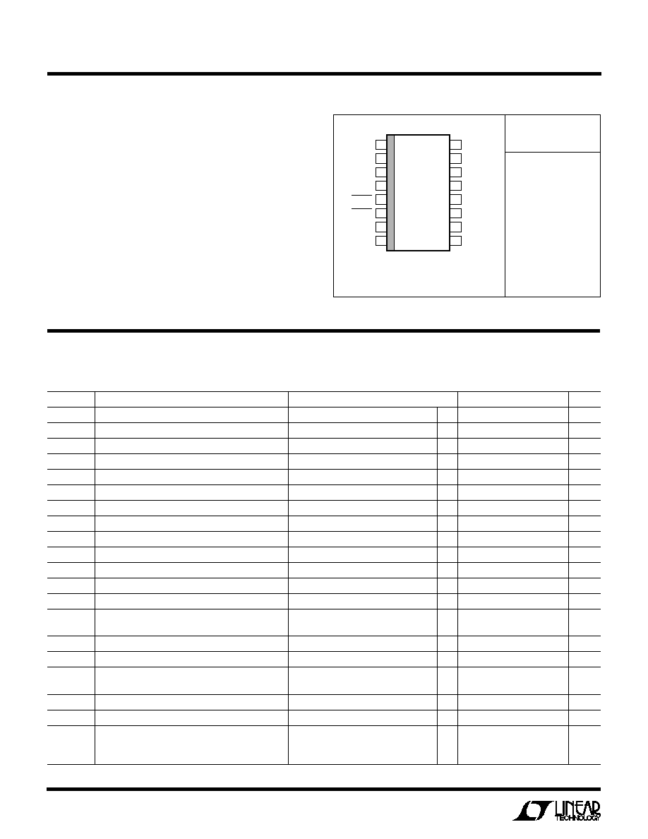
PACKAGE/ORDER I FOR ATIO
U
U
W
(Note 1)
ORDER PART
NUMBER
LTC1642CGN
LTC1642IGN
Consult factory for Military grade parts.
T
JMAX
= 150
∞
C,
JA
= 130
∞
C/W
1
2
3
4
5
6
7
8
TOP VIEW
16
15
14
13
12
11
10
9
CRWBR
BRK TMR
RST TMR
ON
RESET
FAULT
FB
GND
V
CC
SENSE
GATE
REF
COMP
≠
COMP
+
COMPOUT
OV
GN PACKAGE
16-LEAD PLASTIC SSOP
DC ELECTRICAL CHARACTERISTICS
SYMBOL
PARAMETER
CONDITIONS
MIN
TYP
MAX
UNITS
I
CC
V
CC
Supply Current
ON = V
CC
q
1.25
3.0
mA
V
LKHI
V
CC
Undervoltage Lockout (Low to High)
q
2.55
2.73
2.95
V
V
LKLO
V
CC
Undervoltage Lockout (High to Low)
q
2.35
2.50
2.80
V
V
LKHYST
V
CC
Undervoltage Lockout Hysteresis
230
mV
V
CC
Operating Voltage Range
2.97
16.5
V
V
FB
FB Pin Voltage Threshold (FB Falling)
q
1.208
1.220
1.232
V
V
FB
FB Pin Threshold Line Regulation
2.97V
V
CC
16.5V
q
5
15
mV
V
FBHST
FB Pin Voltage Threshold Hysteresis
3
mV
V
OV
OV Pin Voltage Threshold (OV Rising)
q
1.208
1.220
1.232
V
V
OV
OV Pin Threshold Line Regulation
2.97V
V
CC
16.5V
q
5
15
mV
V
OVHYST
OV Pin Voltage Theshold Hysteresis
3
mV
V
RST
RST TMR Pin Voltage Threshold (RST TMR Rising)
q
1.200
1.220
1.250
V
V
RST
RST TMR Pin Threshold Line Regulation
2.97V
V
CC
16.5V
q
5
15
mV
I
RST
RST TMR Pin Current
Timer On
q
≠ 2.5
≠2.0
≠1.5
µ
A
Timer Off, V
RSTTMR
= 1.5V
10
mA
V
BRK
BRK TMR Pin Voltage Threshold (BRK TMR Rising)
q
1.200
1.220
1.250
V
V
BRK
BRK TMR Pin Threshold Line Regulation
2.97V
V
CC
16.5V
q
5
15
mV
I
BRK
BRK TMR Pin Current
Timer On
q
≠ 30
≠20
≠15
µ
A
Timer Off, V
BRKTMR
= 1.5V
10
mA
V
CR
CRWBR Pin Voltage Theshold
q
375
410
425
mV
V
CR
CRWBR Pin Threshold Line Regulation
2.97V
V
CC
16.5V
q
4
15
mV
I
CR
CRWBR Pin Current
CRWBR On, V
CRWBR
= 0V
q
≠ 60
≠ 45
≠ 30
µ
A
CRWBR On, V
CRWBR
= 2.1V
q
≠1500
≠1000
µ
A
CRWBR Off, V
CRWBR
= 1.5V
2.3
mA
The
q
denotes the specifications which apply over the full operating temperature range, otherwise specifications are at T
A
= 25
∞
C.
V
CC
= 5V unless otherwise specified.
3
LTC1642
V
CB
Circuit Breaker Trip Voltage
V
CB
= (V
CC
≠ V
SENSE
), V
FB
= GND
q
15
25
36
mV
V
CB
= (V
CC
≠ V
SENSE
), V
FB
= 1V
q
45
52.5
60
mV
I
CP
GATE Pin Output Current
Charge Pump On, V
GATE
= GND
q
≠ 30
≠ 25
≠ 20
µ
A
Charge Pump Off, V
GATE
= 5V
10
mA
V
GATE
External N-Channel Gate Drive
V
GATE
≠ V
CC,
V
CC
= 3V
q
4.5
5.9
8.0
V
V
GATE
≠ V
CC,
V
CC
= 5V
q
10
11.5
14
V
V
GATE
≠ V
CC,
V
CC
= 15V
q
4.5
8.5
18
V
V
ONHI
ON Pin Threshold (Low to High)
1.30
1.34
1.38
V
V
ONLO
ON Pin Threshold (High to Low)
q
1.20
1.22
1.26
V
V
ONHYST
ON Pin Hysteresis
110
mV
V
OL
Output Low Voltage
RESET, FAULT, COMPOUT I
O
= 1.5mA
q
0.4
V
I
PU
Logic Output Pull-Up Current
RESET, FAULT = GND
≠ 15
µ
A
V
REF
Reference Output Voltage
No Load
q
1.208
1.220
1.232
V
V
LNR
Reference Line Regulation
2.97V
V
CC
16.5V, No Load
q
5
15
mV
V
LDR
Reference Load Regulation
I
O
= 0mA to ≠1mA, Sourcing Only
q
2.5
7.5
mV
I
RSC
Reference Short-Circuit Current
V
REF
= 0V
4.5
mA
V
COS
Comparator Offset Voltage
V
CM
= V
REF
q
±
10
mV
V
CHYST
Comparator Hysteresis
V
CM
= V
REF
3
mV
DC ELECTRICAL CHARACTERISTICS
The
q
denotes the specifications which apply over the full operating temperature range, otherwise specifications are at T
A
= 25
∞
C.
V
CC
= 5V unless otherwise specified.
SYMBOL
PARAMETER
CONDITIONS
MIN
TYP
MAX
UNITS
Note 1: Absolute Maximum Ratings are those values beyond which the life
of a device may be impaired.
PI FU CTIO S
U
U
U
CRWBR (Pin 1): Combination Overvoltage Timer and
Crowbar Circuit Trigger. The timer sets the overvoltage
time needed to trigger the crowbar circuit. To use the timer
connect a capacitor C to ground; the trigger time is
9ms∑C(
µ
F). When the timer is off an internal N-channel
pulls the pin to ground. The timer is started when the OV
comparator trips. A 45
µ
A current source is connected
from V
CC
to the CRWBR pin, and the voltage increases at
a rate of 45/C(
µ
F) Volts/second. When the voltage reaches
410mV the current sourced by the pin increases to 1.5mA.
Boost this current with an NPN emitter follower to trigger
a crowbar SCR.
BRK TMR (Pin 2): Analog Timer which Limits the Time the
Part Remains In Current Limit. To use the timer connect a
capacitor from BRK TMR to ground. BRK TMR is pulled to
ground until the sense resistor current reaches its limit,
when the pin begins sourcing 20
µ
A and the pin voltage
increases at a rate of 20/C(
µ
F) Volts/second. When the pin
reaches 1.23V the GATE pin is pulled to ground and the
FAULT output is asserted until the chip is reset. To allow
the part to remain in current limit indefinitely ground BRK
TMR.
RST TMR (Pin 3): Analog System Timer. To use the timer
connect a capacitor from RST TMR to ground. This timer
sets the delay from the ON pin going high to the start of the
GATE pin's ramp; it also sets the delay from output voltage
good, as sensed by the FB pin, to RESET going high. When
the timer is off, an internal N-channel shorts RST TMR to
ground. When the timer is turned on a 2
µ
A current from
V
CC
is connected and the RST TMR pin voltage starts to
ramp up at a rate of 2/C(
µ
F) Volts/second. The timer trips
when the voltage reaches 1.23V.
4
LTC1642
ON (Pin 4): Control. When ON is low the GATE pin is
grounded and FAULT goes high. The GATE pin voltage
starts ramping up one RST TMR timing cycle after ON
goes high. Pulsing the ON pin low for at least 2
µ
s also
resets the chip when it latches off after a sustained
overvoltage or current limit. The threshold on a low to high
transition is 1.34V with 110mV of hysteresis.
RESET (Pin 5): Open Drain Output. RESET is pulled low if
the voltage at the FB pin is below its trip point and goes
high one timing cycle after the FB voltage exceeds its trip
point plus 3mV of hysteresis. RESET has a weak pull-up to
one diode drop below V
CC
; an external resistor can pull the
pin above V
CC
.
FAULT (Pin 6): Open Drain Output. FAULT is pulled low
when the part latches itself off following a sustained
overvoltage or current limit. It goes high 2
µ
s after the ON
pin goes low. FAULT has a weak pull-up to one diode drop
below V
CC
; an external resistor can pull the pin above V
CC
.
FB (Pin 7): Noninverting Input to An Analog Comparator;
the inverting input is tied to the 1.23V internal reference.
The FB comparator can be used with an external resistive
divider to monitor the output supply voltage. When the FB
voltage is lower than 1.23V the RESET pin is pulled low.
RESET goes high one system timing cycle after the voltage
at FB exceeds its threshold by 3mV of hysteresis. A low
pass filter at the comparator's output prevents negative
voltage glitches from triggering a false reset.
GND (Pin 8): Chip Ground.
OV (Pin 9): Analog Input Used to Monitor Overvoltages.
When the voltage on OV exceeds its trip point the GATE pin
is pulled low immediately and the CRWBR timer starts. If
OV remains above its trip point (minus 3mV of hysteresis)
long enough for CRWBR to reach its trip point the part
latches off until reset by pulsing the ON pin low; otherwise,
the GATE pin begins ramping up one RST TMR timing
cycle after OV goes below its trip point.
COMPOUT (Pin 10): Uncommitted Comparator's Open
Drain Output.
COMP
+
(Pin 11): Uncommitted Comparator's Noninvert-
ing Input.
COMP
≠
(Pin 12): Uncommitted Comparator's Inverting
Input.
REF (Pin 13): The Reference Voltage Output, 1.232V
±
2%. To ensure stability the pin should be bypassed with
a 0.1
µ
F compensation capacitor. For V
CC
= 5V it can
source 1mA.
GATE (Pin 14): High Side Gate Drive for the External
N-Channel. An internal charge pump provides at least 4.5V
of gate drive, but can only source 25
µ
A. The pin requires
an external series RC network to ground to compensate
the current limit loop, and to limit the maximum voltage
ramp which is dV/dt (V/s) = 25/C(
µ
F). GATE is immediately
pulled to ground when the overvoltage comparator trips or
the input supply is below the undervoltage lockout trip
point. During current limit the GATE voltage is adjusted to
maintain constant load current until the BRK TMR pin
trips, when the pin is pulled to ground until the chip is
reset.
SENSE (Pin 15): Current Limit Set. To use the current limit
place a sense resistor in the supply path between V
CC
and
SENSE. Should the drop across the resistor exceed a
threshold voltage the GATE pin is adjusted to maintain a
constant load current and the timer at the BRK TMR pin is
started. To protect the external FET from thermal damage
the circuit breaker trips after the BRK TMR timing cycle. A
foldback feature makes the current limit decrease as the
voltage at FB approaches ground. Figure 3 quantifies the
relationship. To disable the current limit short SENSE to
V
CC
.
V
CC
(Pin 16): Positive Supply Voltage; between 2.97V and
16.5V in normal operation. An internal undervoltage lock-
out circuit holds the GATE pin at ground until V
CC
exceeds
2.73V. If V
CC
exceeds 16.5V an internal shunt regulator
protects the chip from V
CC
and SENSE pin voltages up to
33V. When the internal shunt regulator is active and the
charge pump is on the GATE pin voltage will usually be low
but this is not guaranteed; use the OV pin to ensure that the
pass device is off. The V
CC
pin also provides a Kelvin
connection to the high side of the SENSE resistor.
PI FU CTIO S
U
U
U
5
LTC1642
APPLICATIO S I FOR ATIO
W
U
U
U
Hot Circuit Insertion
When a circuit board is inserted into a live backplane its
supply bypass capacitors can draw large currents from the
backplane power bus as they charge. These currents can
permanently damage connector pins and can glitch the
backplane supply, resetting other boards in the system.
The LTC1642 limits the charging currents drawn by a
board's capacitors, allowing safe insertion in a live
backplane.
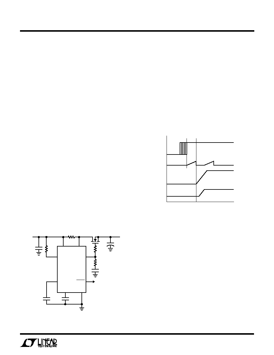
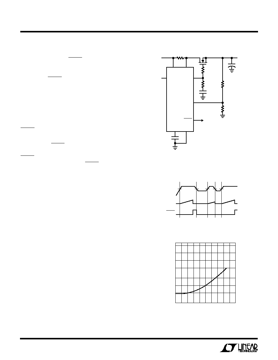
Power Supply Ramping
In the circuit shown in Figure 1 the LTC1642 and the
external N-channel pass transistor Q1 work together to
limit charging currents. When power is first applied to V
CC
the chip holds Q1's gate at ground. After a programmable
delay a 25
µ
A current source begins to charge the external
capacitor C2, generating a voltage ramp of 25
µ
A/C2 V/s at
the GATE pin. Because Q1 acts as a source follower while
its gate ramps, the current charging the board's bypass
capacitance C
LOAD
is limited to 25
µ
A∑C
LOAD
/C2.
An internal charge pump supplies the 25
µ
A gate current,
ensuring sufficient gate drive to Q1. At 3V V
CC
the mini-
mum gate drive is 4.5V; at 5V V
CC
the minimum is 10V; at
15V V
CC
the minimum is again 4.5V, due to a Zener clamp
from the GATE pin to ground. Resistor R3 limits this
Zener's transient current during board insertion and re-
moval and protects against high frequency FET oscilla-
tions.
The delay before the GATE pin voltage begins ramping is
determined by the system timer. It comprises an external
capacitor C1 from the RST TMR pin to ground; an internal
2
µ
A current source feeding RST TMR from V
CC
; an internal
comparator, with the positive input tied to RST TMR and
the negative input tied to the 1.23V reference; and an
NMOS pull-down. In standby, the NMOS holds RST TMR
at ground; when the timer starts the NMOS turns off and
the RST TMR voltage ramps up as the current source
charges the capacitor. When RST TMR reaches 1.23V the
timer comparator trips; the GATE voltage begins ramping
and RST TMR returns to ground. The ramp time
t needed
to trip the comparator is :
t(ms) = 615∑C1(
µ
F).
GATE
ON
14
SENSE
15
RESET
5
4
BRK TMR
2
V
CC
16
R2
0.010
Q1
FDR9410A
GND
LTC1642
8
RST TMR
3
1642 F01
R3
100
R4
330
C2
0.047
µ
F
C
LOAD
+
C7
0.1
µ
F
C1
0.33
µ
F
C4
0.33
µ
F
ALL RESISTORS
±
5% UNLESS NOTED
RESET DELAY = 200ms
SHORT-CIRCUIT DURATION = 20ms
V
IN
12V
2.5A
V
OUT
R1
10k
Figure 1. Supply Control Circuitry
Figure 2. Supply Control Timing
1642 F02
TIME
GATE
SLOPE = 25
µ
A/C(V/s)
RST TMR
V
IN
V
OUT
VOLTS
Powering-Up In Current Limit
Ramping the GATE pin voltage
indirectly limits the charg-
ing current to I = 25
µ
A∑C
LOAD
/C2, where C2 is the external
capacitor connected to the GATE and C
LOAD
is the load
capacitance. If the value of C
LOAD
is uncertain, then a
worst-case design can often result in needlessly long
ramp times, and it may be better to limit the charging
current directly.
Current Limiting and Solid-State Circuit Breaker
The board current can be limited by connecting a sense
resistor between the LTC1642's V
CC
and SENSE pins. An
internal servo loop adjusts the GATE pin voltage such that
Q1 acts as a constant current source if the voltage drop
across the sense resistor reaches a limit. The voltage limit
across the sense resistor increases as the output charges
6
LTC1642
APPLICATIO S I FOR ATIO
W
U
U
U
up; this "foldback" limiting tends to keep the power
dissipation in the N-channel pass transistor constant. The
output voltage is sensed at the FB pin. The limiting sense
resistor voltage is 23mV when FB is grounded, but in-
creases gradually to 53mV when FB exceeds 1V; Figure 3
shows the full dependence.
When the sense resistor voltage reaches its limit, a circuit
breaker timer starts. This timer uses the BRK TMR pin and
has a 1.23V threshold. If BRK TMR reaches 1.23V the
timer comparator trips, tripping the circuit breaker; if the
sense resistor voltage falls below its limit before the
comparator trips the GATE voltage begins ramping back
up immediately. The ramp time
t needed to trip the
comparator is
t(ms) = 62∑C(
µ
F), where C is the external
capacitance.
Once the circuit breaker trips, GATE and FAULT remain at
ground until the chip is restarted. To restart, hold the ON
pin low for at least 2
µ
s and FAULT will go high. Then take
ON high again and the GATE will ramp up after a system
timing cycle. Or, configure the LTC1642 to restart itself
after the circuit breaker trips by connecting FAULT to the
ON pin.
The servo loop controlling Q1 during current limit has a
unity-gain frequency of about 125kHz; in Figure 1 R4,
together with C2, provide compensation. To ensure stabil-
ity the product 1/(2∑
∑R4∑C2) should be kept below the
unity-gain frequency, and C2 should be more than Q1's
gate-source capacitance. The values shown in Figure 1,
0.047
µ
F and 330
, are a starting point.
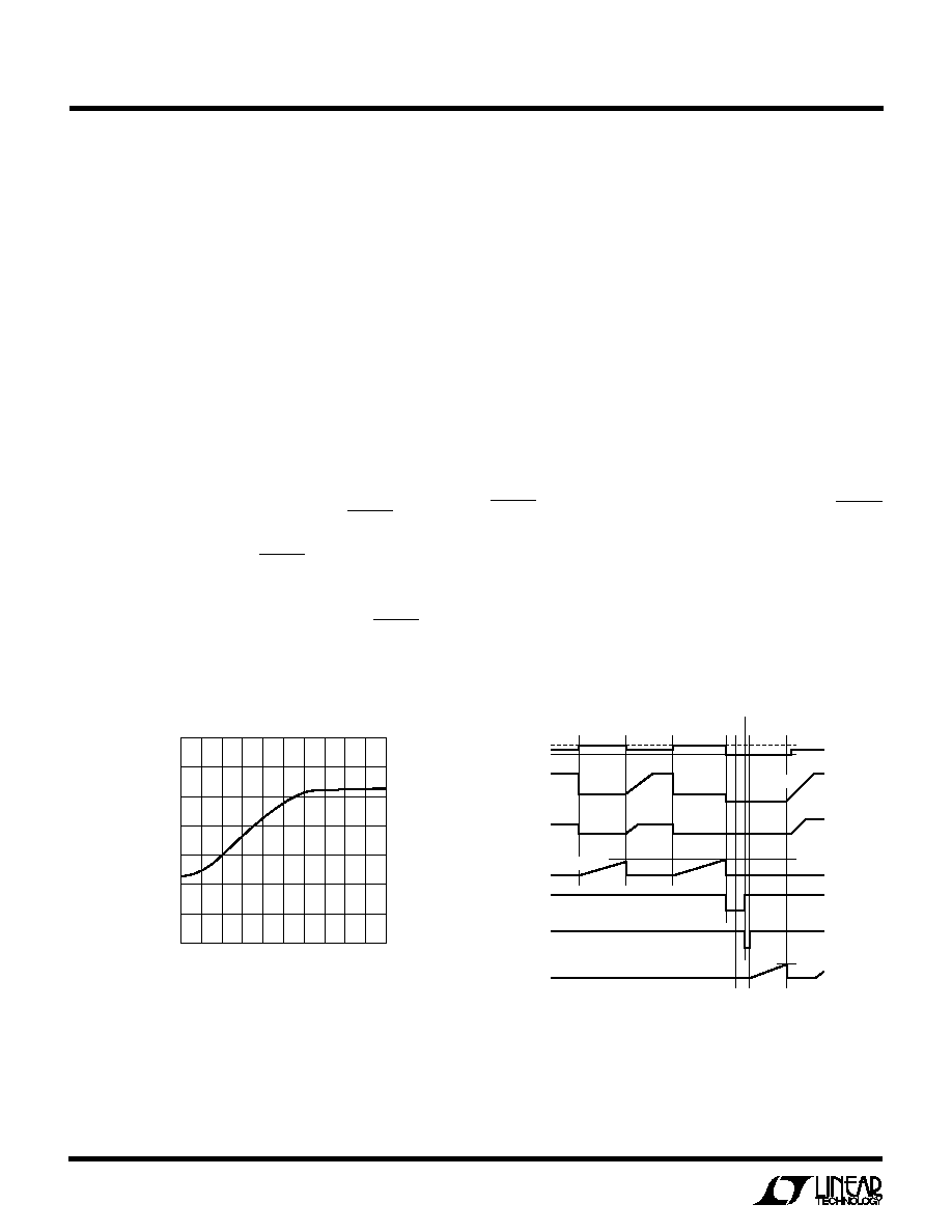
Typical waveforms during a load short to ground are
shown in Figure 4. The load is shorted to ground at time 1.
The GATE voltage drops until the load current equals its
maximum limit, and the circuit breaker timer starts. The
short is cleared at time 2, before the timer trips. The BRK
TMR pin returns to ground, and the GATE voltage begins
ramping up. At time 3 the load is shorted again and at time
4 the timer trips, pulling the GATE to ground and asserting
FAULT. Although the short is cleared at time 5, FAULT
doesn't go high until the ON pin is pulled low at time 6. At
time 7 ON goes high and the system timer starts. When it
trips at time 8 the GATE voltage begins ramping.
FB PIN VOLTAGE (mV)
0 100 200 300 400 500 600 700 800 900 1000
MAXIMUM SENSE RESISTOR VOLTAGE (mV)
1642 F03
70
60
50
40
30
20
10
0
Figure 3. Maximum Sense Resistor Voltage vs FB Voltage
I
LOAD
GATE
I
LIMIT
1.23V
V
OUT
6
7
5
4
3
2
1
8
GATE
BRK TMR
RST TMR
ON
0A
1.23V
1642 F04
FAULT
Figure 4. Current Limit and Circuit Breaker Timing

7
LTC1642
APPLICATIO S I FOR ATIO
W
U
U
U
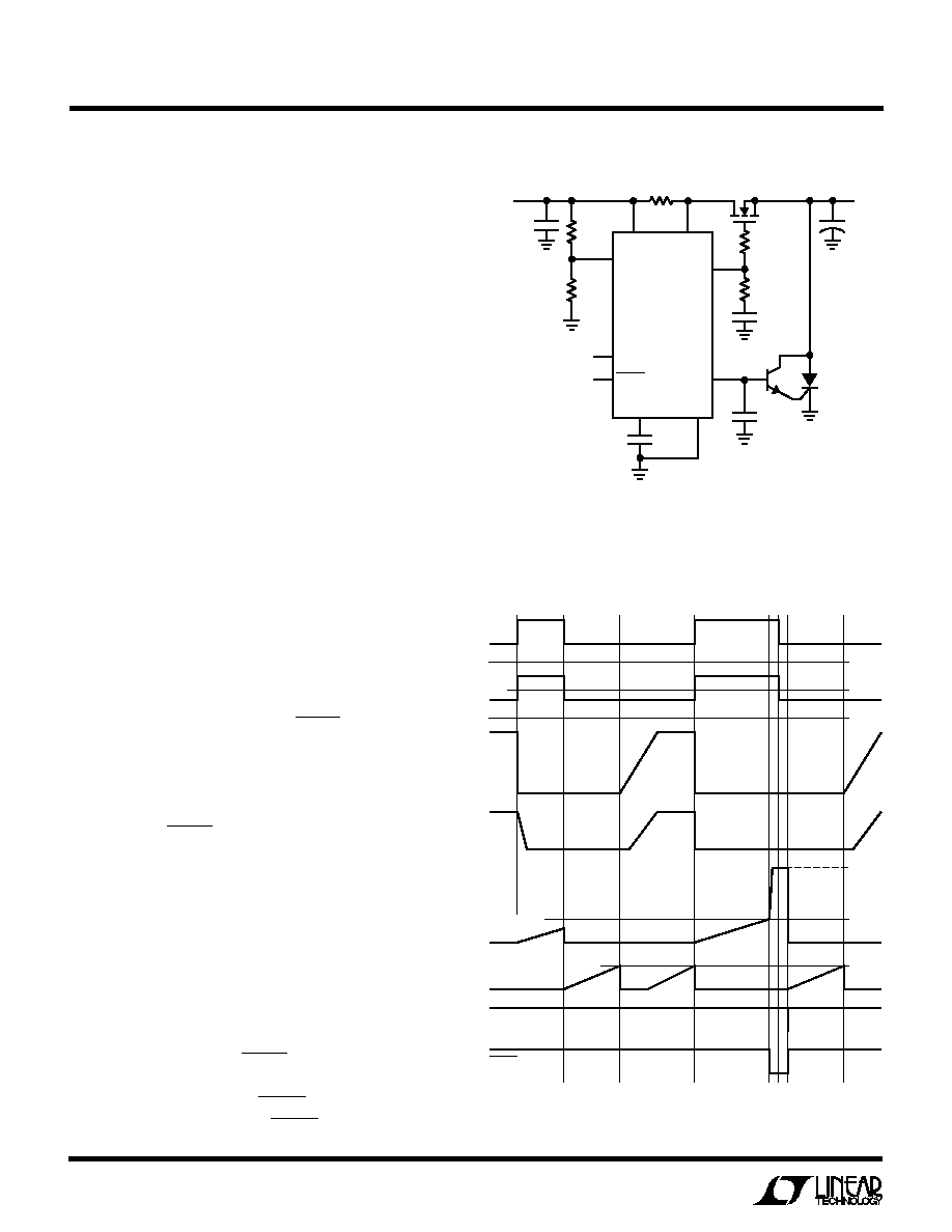
Automatic Restart After a Current Fault
The LTC1642 will automatically attempt to restart itself
after the circuit breaker opens if the FAULT output is tied
to the ON pin. The circuit is shown in Figure 5, and the
waveforms during a load short in Figure 6.
During a continuous current limit such as a load short, the
N-channel pass transistor's duty cycle is equal to the
circuit breaker timer period, divided by the sum of the
circuit breaker and system timer periods. If FAULT is tied
to ON then open drain logic should be used to drive the
node. The external pull-up resistor at the ON pin may be
omitted because FAULT provides a weak pull-up.
Undervoltage Lockout
An internal undervoltage lockout circuit holds the charge
pump off until V
CC
exceeds 2.73V. If V
CC
falls below 2.5V,
it turns off the charge pump and clears overvoltage and
current limit faults.
For higher lockout thresholds tie the ON pin to a resistor
divider driven from V
CC
, as shown in Figure 7. This
circuit keeps the charge pump off until V
CC
exceeds
(1+R1/R5)∑1.34V, and also turns it off if V
CC
falls below
(1+R1/R5)∑1.23V.
GATE
14
SENSE
15
ON
4
V
CC
16
R2
0.010
Q1
FDR9410A
GND
LTC1642
8
RST TMR
3
R1
464k
1%
R5
60.4k
1%
V
IN
12V
2.5A
1642 F07
R3
100
R4
330
C2
0.047
µ
F
+
C7
0.1
µ
F
C1
0.33
µ
F
ALL RESISTORS
±
5% UNLESS NOTED
V
OUT
UNDERVOLTAGE
LOCKOUT
THRESHOLD = 10.7V
C
LOAD
Figure 7. Setting a Higher Undervoltage Lockout
6
5
4
3
2
1
BRK TMR
1.23V
1.23V
1642 F06
GATE
V
OUT
RST TMR
ON/FAULT
GATE
ON
14
SENSE
15
CRWBR
1
4
FAULT
6
OV
BRK TMR
2
9
V
CC
16
R2
0.010
Q1
FDR9410A
GND
LTC1642
8
RST TMR
3
R5
1642 F05
R3
100
R4
330
C2
0.047
µ
F
+
C7
0.1
µ
F
C1
0.33
µ
F
C4
0.33
µ
F
ALL RESISTORS
±
5% UNLESS NOTED
Q2
2N2222
Q3
MCR
12DC
C5
V
IN
12V
2.5A
V
OUT
R1
C4
C4 + 10 ∑ C1
SHORT-CIRCUIT DUTY CYCLE =
= 9%
C
LOAD
Figure 5. Automatic Restart Circuit
Figure 6. Automatic Retry Following a Load Short
8
LTC1642
Overvoltage Protection
The LTC1642 can protect a load from overvoltages by
turning off the pass transistor if the supply voltage ex-
ceeds a programmable limit, and by triggering a crowbar
SCR if the overvoltage lasts longer than a programmable
time. The part can also be configured to automatically
restart when the overvoltage clears.
The overvoltage protection circuitry is shown in Figure 8.
The external components comprise a resistor divider
driving the OV pin, timing capacitor C5, NPN emitter
follower Q2, and crowbar SCR Q3. Because the MCR12DC
is not a sensitive-gate device, the optional resistor shunt-
ing the SCR gate to ground is omitted. The internal
components comprise a comparator, 1.23V bandgap ref-
erence, two current sources, and a timer at the CRWBR
pin. When V
CC
exceeds (1+R1/R5)∑1.23V the comparator's
output is high and internal logic pulls the GATE down and
starts the timer. This timer has a 0.410V threshold and
uses the CRWBR pin; when CRWBR reaches 0.410V the
timer comparator trips, and the current sourced from V
CC
increases to 1.5mA. Emitter follower Q2 boosts this cur-
rent to trigger crowbar SCR Q3. The ramp time
t needed
to trip the comparator is :
t(ms) = 9.1∑C5(
µ
F).
Once the CRWBR timer trips the LTC1642 latches off: after
the overvoltage clears GATE and FAULT remain at ground
and CRWBR continues sourcing 1.5mA. To restart the part
after the overvoltage clears, hold the ON pin low for at least
2
µ
s and then bring it high. The GATE voltage will begin
ramping up one system timing cycle later. The part will
restart itself if FAULT and ON are connected: GATE begins
ramping up one system timing cycle after the overvoltage
clears.
Figure 9 shows typical waveforms when the divider is
driven from V
CC
. The OV comparator goes high at time 1,
causing the chip to pull the GATE pin to ground and start
the CRWBR timer. At time 2, before the timer's compara-
tor trips, OV falls below its threshold; the timer resets and
GATE begins charging one system timing cycle later at
time 3. Another overvoltage begins at time 4, and at time
5 the CRWBR timer trips; FAULT goes low and the CRWBR
pin begins sourcing 1.5mA. Even after OV falls below
1.23V at time 6, GATE and FAULT stay low, and CRWBR
continues to source 1.5mA. FAULT goes high when ON
GATE
ON
14
SENSE
15
CRWBR
1
4
FAULT
6
OV
9
V
CC
16
R2
0.010
Q1
FDR9410A
GND
LTC1642
8
RST TMR
3
R1
127k
1%
R5
12.4k
1%
V
IN
12V
2.5A
1642 F08
R3
100
R4
330
C2
0.047
µ
F
+
C7
0.1
µ
F
C1
0.33
µ
F
ALL RESISTORS
±
5% UNLESS NOTED
OV COMPARATOR TRIPS AT V
IN
= 13.85V
RESET TIME = 200ms
CROWBAR DELAY TIME = 90
µ
s
Q2
2N2222
Q3
MCR12DC
C5
0.01
µ
F
V
OUT
C
LOAD
Figure 8. Overvoltage Protection Circuitry
1642 F09
1.23V
0.41V
V
CC
0V
0V
1.23V
GATE
0V
V
CC
V
OUT
OV
6 7
8
5
4
3
2
1
CRWBR
RST TMR
ON
FAULT
Figure 9. Overvoltage Timing (High Side)
APPLICATIO S I FOR ATIO
W
U
U
U
9
LTC1642
The OV and FB Comparators
The propagation delay through the OV and FB compara-
tors on low to high transitions depends strongly on the
differential input voltage. The relationship is shown in
Figure 11. The minimum propagation delay for large
overdrives is about 20
µ
s. In addition the comparators
have 3mV of hysteresis.
Internal Voltage Clamp Protection
The LTC1642 includes a shunt regulator to protect itself
from V
CC
and SENSE pin voltages up to 33V. The regulator
turns on when V
CC
exceeds 16.5V and limits most of the
chip's circuitry to 15V. When it is on the chip functions
normally with one exception: if the charge pump is on, the
GATE voltage is usually near ground but this is not
guaranteed. Use the OV pin to ensure that GATE is grounded.
The pull-up voltage on the RESET and FAULT pins follows
V
CC
until the shunt regulator turns on. When the regulator
is on the pull-up voltage is 14.4V.
goes low at time 7, and GATE begins charging at time 8,
one RST TMR cycle after FAULT goes high.
Figure 10 shows typical waveforms when the OV divider is
driven from the N-channel's low side. Because the voltage
driving the divider collapses after the OV comparator trips,
FAULT stays high and CRWBR stays near ground, which
prevents the pin from triggering an SCR. The GATE voltage
begins ramping up after a RST TMR timing cycle.
Automatic Restart
If there is an overvoltage, and the resistor divider feeding
OV is connected to the output of the N-channel pass
transistor, the LTC1642 will automatically restart even if
FAULT is not tied to ON. If the divider is connected to the
input side, the LTC1642 will restart itself only if FAULT is
tied to ON, and only after the overvoltage clears.
APPLICATIO S I FOR ATIO
W
U
U
U
0V
0V
0.41V
1.23V
1.23V
1642 F10
6 7
5
4
3
2
1
GATE
V
OUT
V
CC
OV
RST TMR
FAULT
0V
CRWBR
Figure 10. Overvoltage Timing (Low Side)
OV OVERDRIVE (mV)
0
40
80
120
160
200
240
OV COMPARATOR PROPAGATION DELAY (
µ
s)
1642 F11
70
60
50
40
30
20
10
0
Figure 11. OV Comparator Propagation Delay vs
Overdrive Voltage
10
LTC1642
APPLICATIO S I FOR ATIO
W
U
U
U
Undervoltage Monitor
The LTC1642 will assert RESET if a monitored voltage falls
below a programmable minimum. When the monitored
voltage has exceeded its minimum for at least one system
timing cycle, RESET goes high. The monitoring circuitry
comprises an internal 1.23V bandgap reference, an inter-
nal precision voltage comparator and an external resistive
divider to monitor the output supply voltage. The circuit is
shown in Figure 12, and typical waveforms in Figure 13.
When the voltage at the FB pin rises above its reset
threshold (1.23V), the comparator output goes low and a
timing cycle starts (times 1 and 5). Following the cycle
RESET is pulled high.
At time 2 the voltage at FB drops below the comparator's
threshold and RESET is pulled low. If the FB pin rises
above the reset threshold for less than a timing cycle the
RESET output will remain low (time 3 to time 4). The 15
µ
A
pull-up current source to V
CC
on RESET has a series diode
so the pin can be pulled above V
CC
by an external pull-up
resistor without forcing current back into the supply.
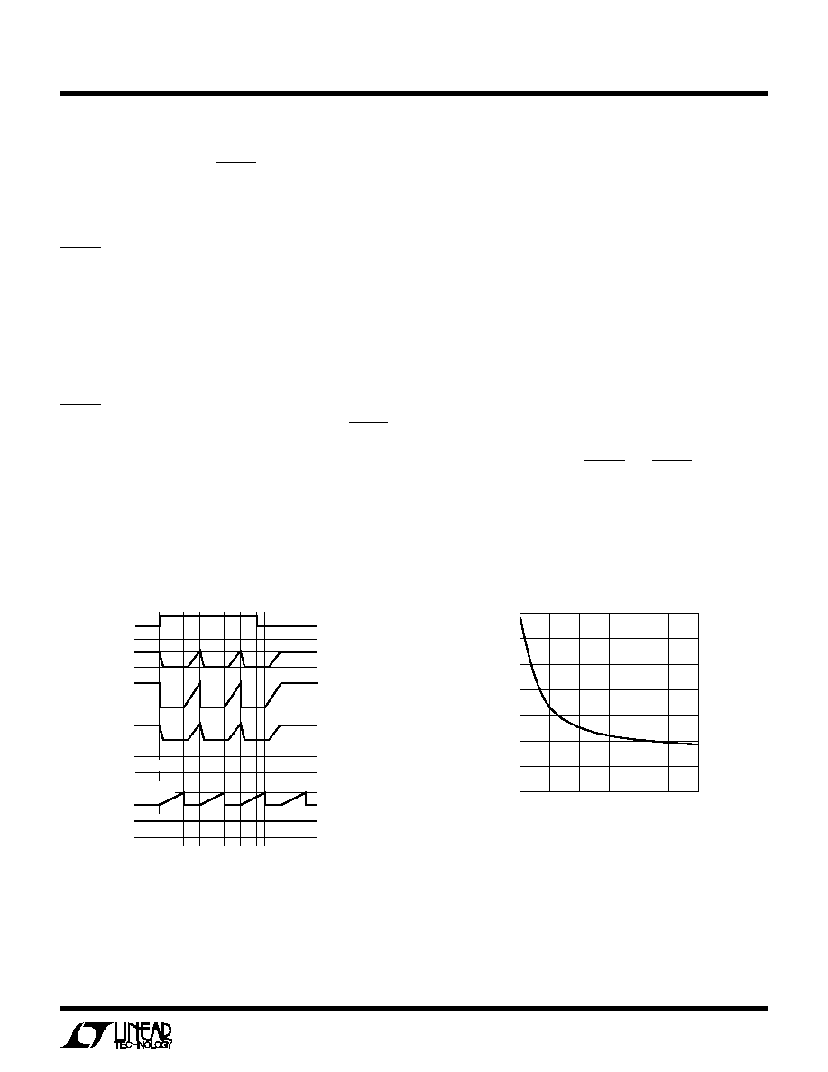
Reference
The LTC1642's internal voltage reference is buffered and
brought out to the REF pin. The buffer amplifier should be
compensated with a capacitor connected between REF
and ground. If no DC current is drawn from REF, 0.1
µ
F
ensures an adequate phase margin, but the minimum
compensation increases if REF sources a substantial DC
current, as shown in Figure 14.
Uncommitted Comparator
The uncommitted comparator has an open drain output.
The comparator has 3mV of hysteresis: the output goes
high when the differential input voltage exceeds 1.5mV
and goes low when the differential input is less than
≠1.5mV.
GATE
ON
14
SENSE
15
FB
7
RESET
5
4
V
CC
16
R2
0.010
Q1
FDR9410A
GND
LTC1642
8
RST TMR
3
1642 F12
R3
100
R4
330
C2
0.047
µ
F
R7
95.3k
1%
R6
12.4k
1%
+
C1
0.33
µ
F
ALL RESISTORS
±
5% UNLESS NOTED.
FB COMPARATOR TRIPS AT V
OUT
= 10.7V
V
IN
12V
2.5A
V
OUT
C
LOAD
Figure 12. Undervoltage Monitoring Circuitry
1642 F13
V
OUT
RST TMR
V1
V2
V2
V1
5
4
3
2
1
RESET
V1
Figure 13. Supply Monitor Waveforms
REFERENCE CURRENT
100
µ
A
1mA
10mA
MINIMUM REF COMPENSATION (
µ
F)
1642 F14
0.1
0.2
0.4
1.0
2.0
4.0
10.0
Figure 14. Minimum REF Compensation vs REF Current
11
LTC1642
Dimensions in inches (millimeters) unless otherwise noted.
PACKAGE DESCRIPTIO
U
GN Package
16-Lead Plastic SSOP (Narrow 0.150)
(LTC DWG # 05-08-1641)
GN16 (SSOP) 0398
* DIMENSION DOES NOT INCLUDE MOLD FLASH. MOLD FLASH
SHALL NOT EXCEED 0.006" (0.152mm) PER SIDE
** DIMENSION DOES NOT INCLUDE INTERLEAD FLASH. INTERLEAD
FLASH SHALL NOT EXCEED 0.010" (0.254mm) PER SIDE
1
2
3
4
5
6
7
8
0.229 ≠ 0.244
(5.817 ≠ 6.198)
0.150 ≠ 0.157**
(3.810 ≠ 3.988)
16 15 14 13
0.189 ≠ 0.196*
(4.801 ≠ 4.978)
12 11 10 9
0.016 ≠ 0.050
(0.406 ≠ 1.270)
0.015
±
0.004
(0.38
±
0.10)
◊
45
∞
0
∞
≠ 8
∞
TYP
0.007 ≠ 0.0098
(0.178 ≠ 0.249)
0.053 ≠ 0.068
(1.351 ≠ 1.727)
0.008 ≠ 0.012
(0.203 ≠ 0.305)
0.004 ≠ 0.0098
(0.102 ≠ 0.249)
0.025
(0.635)
BSC
0.009
(0.229)
REF
12
LTC1642
©
LINEAR TECHNOLOGY CORPORATION 1999
1642is, sn1642 LT/TP 0599 4K ∑ PRINTED IN USA
RELATED PARTS
PART NUMBER
DESCRIPTION
COMMENTS
LTC1421
Hot Swap Controller
Multiple Supplies
LTC1422
Hot Swap Controller
Single Supply in SO-8
LT1640
Negative Voltage Hot Swap Controller
Negative High Voltage Supplies
LTC1643
PCI-Bus Hot Swap Controller
3.3V, 5V, 12V, ≠12V Supplies for PCI Bus
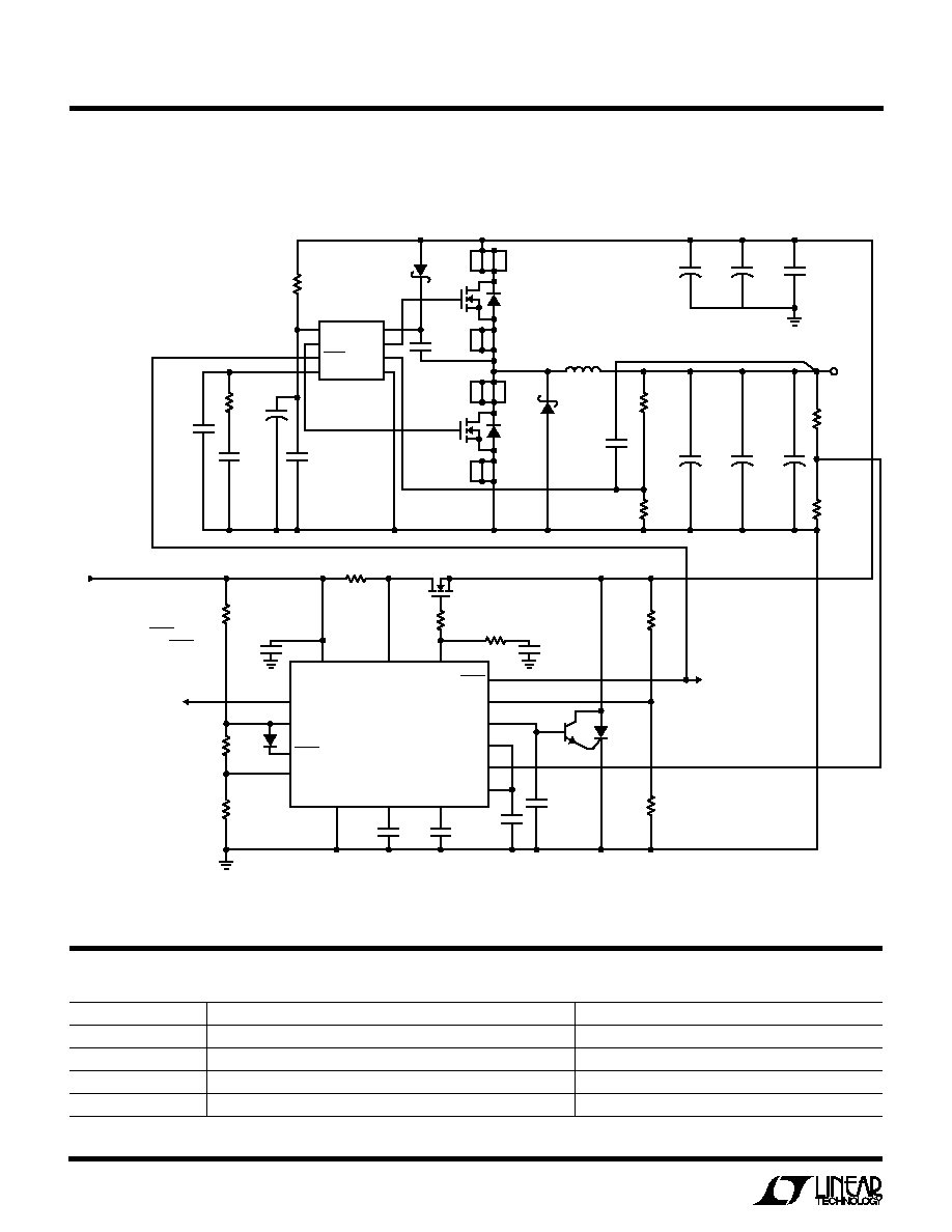
TYPICAL APPLICATIO
U
Linear Technology Corporation
1630 McCarthy Blvd., Milpitas, CA 95035-7417
(408) 432-1900
q
FAX: (408) 434-0507
q
www.linear-tech.com
PV
CC2
G2
SHDN
COMP
PV
CC1
G1
FB
GND
7
8
5
6
2
1
4
3
U2
LTC1430CS
Q4
Si4412DY
L1
3.5
µ
H
CDRH1273R5
Q5
Si4412DY
5V
V
CC
SENSE
GATE
GND
BRK TMR
U1
LTC1642
RST TMR
16
15
14
8
2
3
COMPOUT
ON
FAULT
OV
10
4
6
9
RESET
FB
CRWBR
COMP
+
REF
COMP
≠
5
7
1
11
13
12
C3
0.33
µ
F
C2
0.33
µ
F
C4
0.1
µ
F
Q2
2N2222
Q3
MCR
12DC
R6
2.55k
1%
D3
1N4148
R5
36.5k
1%
R10
12k
C14
2200pF
R11
16.5k
1%
R12
10.2k
1%
R2
100
R3
32.4k
1%
R4
13k
1%
Q1
MTB50N06V
C5
0.01
µ
F
C1
47nF
C6
0.1
µ
F
R8
330
R7
11.3k
1%
5V POWER-GOOD = 4.75V
3.3V POWER-GOOD = 3.00V
1642 TA02
LATCH OFF: FLOAT FAULT
AUTOMATIC RETRY: TIE FAULT TO ON
ALL RESISTORS 5% UNLESS OTHERWISE NOTED
RESET TIME = 200ms
CURRENT LIMIT TIME =20ms
CROWBAR TIME = 90
µ
s
UNDERVOLTAGE = 4.49V
OVERVOLTAGE = 5.47V
R1, 0.005
C7
0.1
µ
F
D1
MBRS130T3
C9
270pF
C8
15
µ
F
10V
KEMET
TANT
+
5 6 7 8
1 2 3
5
4
4
6 7 8
1 2 3
C15
0.1
µ
F
D2
MBR0530T1
C18
680pF
C10
330
µ
F
6.3V
KEMET
TANT
+
C11
330
µ
F
6.3V
KEMET
TANT
+
C12
330
µ
F
6.3V
KEMET
TANT
+
C16
330
µ
F
6.3V
KEMET
TANT
+
C17
330
µ
F
6.3V
KEMET
TANT
+
C13
1
µ
F
R13
17.4k
1%
3.3V
OUT
AT 5A
R14
12.1k
1%
R9
51
5V To 3.3V Hot Swap Supply Using the LTC1430